


Samsung Foundry, which is the production wing of Samsung, has launched a brand new production process of its seven-nanometer Lower Power Plus process node. According to an official press statement, this new device could lower the energy consumption by nearly 50%.
How It Would Benefit The Miners
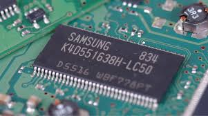
This new process has been entirely based on the EUV –The Extreme Ultraviolet Lithography Technology. This feature makes the seven-nanometer Low Power Plus process node more energy efficient and area efficient due to its density. This could be beneficial to Cryptocurrency miners that are using the new hardware designed by Samsung. One of the most critical factors in the profitability of the industry is the cost of energy, and so this can greatly help. The mining hardware market is one of the few that has witnessed great growth over the past few months.
Mining hardware continue to develop at a pace that is more rapid compared to other markets. And with these new developments, chips have continued to become not only efficient but also smaller in size. It can be remembered that barely six months ago, Samsung developed ten-nanometer hardware that was going to be used by the DragonMint T1 for Halong Mining.
Now, they have developed the new EUV-based 7 Low Power Plus process node that is set to change a lot in the industry. This new development is a great push for the roadmap of Samsung Foundry technology. There are also possibilities that this new development could pave the way for the manufacture of a new three-nanometer technology node semiconductor.
AI Technological Push
Artificial Intelligence is one of the old technologies that have been reinvented by several technological companies in the past. According to the official statement released by Samsung, the seven-LPP will allow the technological push of technologies such as Internet of Things {IoT}, Artificial Intelligence, enterprise and hyperscale datacenter, 5G, automotive and networking. Whereas the names of the first customers that used the new 7LPP mining technology were not disclosed by Samsung, the company suggested that the first chips to apply it would target High Performance Computing and mobile applications.
This Is A Revolutionary Discovery…
 According to the vice president of Samsung Electronics’ foundry sales and marketing team, Charlie Bae, the introduction of the latest EUV-based 7 LPP node is revolutionary breakthrough in the semiconductors market. He has clearly stated that the wafers development fundamental shift will be an optional choice for the mobile and High Performance Computing technology, as well as a wide range of other top-notch applications.
Just barely hours ago, some major predictions were made in regards to the current nature of the market. Taiwan Semiconductor Manufacturing, one of the most established world’s chip manufacturing companies, predicted reduced demands for Cryptocurrency mining hardware. This is expected to counterbalance its revenue growth Q4 2018. But at the moment, the focus will still remain on these new energy efficient chips manufactured by Samsung to the crypto miners.


